Semiconductor Jobs and H-1B Sponsorship in the CHIPS Act Era (2026)
The CHIPS Act is pumping billions into US fabs — and the industry desperately needs international engineers to fill the gap. Here is how to land a sponsored role.
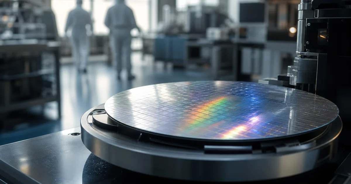
You studied electrical engineering, computer engineering, or materials science. You know how chips are made, or how they are designed. The United States is now spending tens of billions of dollars to build more fabs on home soil — and it is running short of the engineers who actually know how to do that. If you are an international student or professional on F-1, OPT, or H-1B, the current semiconductor build-out is one of the most favorable hiring environments for sponsored employment in recent memory.
The catch is that this sector has its own quirks — security requirements at some employers, a design vs. process/fab distinction, and sponsorship timelines that overlap awkwardly with OPT expiration. This guide covers where the jobs are, which employers sponsor, how the CHIPS Act reshapes your search, and how to move from OPT to a sponsored H-1B in chip design or manufacturing.
What the CHIPS Act actually does for you
The CHIPS and Science Act, signed in 2022 and actively distributing awards through 2025 and 2026, provides approximately $52 billion for domestic semiconductor manufacturing and research. Large recipients include TSMC's Arizona fabs, Intel's Ohio and Arizona expansions, Micron's Idaho and New York facilities, and Samsung's Taylor, Texas plant. Each of these projects requires hundreds to thousands of engineers across process engineering, equipment engineering, yield, design, and R&D functions.
The CHIPS Act does not create a new visa category or change H-1B caps. It does not directly modify immigration rules. What it does is create an enormous workforce demand that US domestic supply cannot meet in the short term — particularly for the highly specialized skills required in leading-edge node manufacturing. Employers receiving CHIPS Act funding are under pressure to hire and ramp quickly, which means they are more willing than in prior cycles to sponsor H-1B petitions for qualified international engineers.
The workforce gap is most acute in:
- Process integration and module engineering for sub-10nm nodes
- Fab equipment engineering (CVD, etch, CMP, lithography)
- Yield and defect analysis engineering
- Chip design roles in analog, mixed-signal, and RF
- VLSI physical design, place-and-route, and verification
If your background touches any of these areas, you are in a structurally advantaged position.
Role categories and which ones sponsor best
Not all semiconductor jobs are equally visa-friendly. The table below gives a practical overview.
| Role Category | Common Titles | H-1B Specialty Occupation | Typical Degree Requirement |
|---|---|---|---|
| Chip Design | RTL Design Engineer, Physical Design Engineer, VLSI Verification Engineer | Strong — well-established | BS/MS EE or CE |
| Process Engineering | Process Integration Engineer, CVD/Etch Engineer, Module Engineer | Strong — clearly technical | BS/MS Materials Sci, ChemE, EE |
| Equipment Engineering | Equipment Engineer, Metrology Engineer | Moderate — sometimes challenged | BS/MS EE, Mechanical, Physics |
| Yield / Failure Analysis | Yield Engineer, Failure Analysis Engineer | Strong | BS/MS EE, Materials |
| RF and Analog Design | RF IC Designer, Analog Design Engineer | Strong | MS/PhD EE preferred |
| Research Scientist | Process R&D Scientist, Materials Scientist | Strong — PhD-level preferred | PhD Materials, Physics, ChemE |
| EDA / CAD Tools | CAD Engineer, EDA Software Engineer | Strong | BS/MS CS, EE |
| Manufacturing / Ops | Manufacturing Engineer, Operations Manager | Moderate | BS/MS Industrial, EE |
For H-1B specialty-occupation purposes, roles requiring a bachelor's degree or higher in a specific technical field qualify more cleanly. USCIS has historically been comfortable with chip design and process engineering roles as specialty occupations. Equipment engineering roles can sometimes draw Requests for Evidence (RFEs) if the employer's job description is vague about the degree requirement — tighter job descriptions help.
Top semiconductor employers that sponsor H-1B
The following companies have strong H-1B sponsorship histories. This list is illustrative, not exhaustive.
Fabless and integrated device manufacturers: NVIDIA (GPU architecture, VLSI), Qualcomm (RF, modem, SoC), AMD (CPU/GPU architecture), Texas Instruments (analog and embedded), Broadcom, and Marvell Technology.
Foundries and IDMs with CHIPS Act expansion: Intel (large H-1B filing volume; process and design), TSMC Arizona (actively scaling process and equipment engineers), Micron Technology (DRAM and NAND process, strong STEM OPT history), Samsung Austin Semiconductor (logic and memory).
Equipment and materials: Applied Materials, Lam Research, KLA Corporation, and ASML (note that some ASML roles carry export-control restrictions — read the job description carefully).
To verify a specific company's sponsorship history, the how to check if a company sponsors H-1B guide walks through the USCIS LCA disclosure data and third-party tools.
ITAR and security clearance — the international student reality
This is where semiconductor differs from most tech sectors. Some roles at defense-adjacent chip companies or government-contracted programs involve ITAR (International Traffic in Arms Regulations) controlled technology or require a US security clearance. ITAR-controlled roles typically cannot be filled by international nationals without an export license, which is rarely granted quickly. Security clearances require US citizenship in almost all cases.
If a job description says "Must be a US Person," "Active Secret clearance required," or "Export Control restrictions apply," that role is not available to F-1 or H-1B holders. Commercial fabs — TSMC Arizona, Micron, Samsung Austin — are generally not ITAR-restricted in their standard engineering roles.
Focus on commercial semiconductor companies: fabless design houses, commercial foundries, equipment makers, and EDA firms. The sector is large enough that you do not need to chase clearance-adjacent roles. The aerospace guide for international students covers where ITAR lines fall across adjacent industries.
Your visa timeline in the semiconductor sector
Here is a realistic timeline for an international student entering a semiconductor role from a May graduation date.
Step-by-step timeline:
- January–March of final academic year: Begin applying to full-time roles. Target May start dates where possible. Get offers signed with OPT authorization confirmed by your DSO before graduation.
- April–May: Graduate. Your OPT application (Form I-765) should already be approved or pending. Standard OPT gives you 12 months of work authorization starting on your requested start date.
- Month 1–6 of OPT: Start working. Your employer's immigration team should initiate the H-1B conversation during this window, not in month 11.
- October–December: Your employer files an H-1B registration during the registration window (typically early March of the following year). Registration, not a full petition.
- Following March: H-1B lottery registration opens. USCIS typically runs the lottery in March–April.
- April–June: If selected, your employer files the full I-129 petition. Apply for STEM OPT extension (Form I-765) immediately if you have a STEM-eligible degree (most semiconductor engineering degrees qualify) and your employer is E-Verify registered.
- October 1: H-1B becomes effective (or April 1 with cap-gap protection under the 2025 H-1B Modernization Rule, if applicable).
If you are not selected in the lottery: Apply for STEM OPT extension immediately. You get 24 additional months (36 total) to attempt the lottery again — but your employer must be E-Verify enrolled and must submit an I-983 training plan. The 90-day unemployment limit applies throughout; track your days carefully. After two failed lottery cycles, review the H-1B backup plans guide for cap-exempt, O-1A, and EB-2 NIW alternatives.
VLSI and chip design roles — maximizing your candidacy
If you are targeting chip design roles specifically, the master's degree (or PhD) level is where most sponsored positions concentrate. Fabless companies like NVIDIA, Qualcomm, and AMD predominantly hire at MS or PhD level for design roles, and the H-1B specialty-occupation argument is straightforward at that credential level.
Specific skills that command attention from sponsors in 2026: RTL design (Verilog, SystemVerilog) with tapeout or class project experience; physical design (Cadence Innovus, Synopsys ICC2) with FinFET or gate-all-around DRC knowledge; UVM or formal verification (Jasper, Questa); analog/mixed-signal simulation in Spectre or HSPICE; DFT (ATPG, boundary scan); and Python or Tcl scripting for EDA automation.
Tailor your resume to demonstrate tapeout experience or academic chip projects (MIT OpenROAD, VLSI course projects, hackathons). Employers sponsoring H-1B for chip design roles want candidates who can contribute to the design cycle quickly — tapeout experience shortens onboarding and makes the sponsorship cost easier to justify.
For broader resume targeting advice, electrical engineer H-1B sponsorship in 2026 has applicable strategies that carry directly into semiconductor design roles.
Fab and process engineering — a different set of signals
Process and fab engineering roles are physically tied to specific locations — Arizona, Ohio, Texas, New York, Idaho — rather than concentrated in Bay Area or Seattle tech clusters. Adjust your geographic expectations accordingly.
Fab employers sponsor candidates who demonstrate lab-based experience in thin film deposition (ALD, CVD, PVD), dry and wet etch, CMP, lithography (193nm or EUV), defect inspection (SEM, TEM, AFM), and statistical process control or DOE methodology. A master's or PhD in materials science, chemical engineering, physics, or EE with a solid-state focus maps directly onto these roles — if your thesis involved semiconductor processing or materials characterization, highlight it explicitly.
TSMC Arizona has been the most visible CHIPS Act beneficiary and recruits through structured campus programs as well as direct applications via their careers portal.
The green card path from semiconductor H-1B
The EB-2 NIW (National Interest Waiver) argument is particularly strong in semiconductors. USCIS has recognized US semiconductor manufacturing capacity as a national interest, and policy guidance from late 2024 cited CHIPS Act priorities as relevant to NIW petitions in manufacturing and materials science.
Your main paths:
- EB-3 or EB-2 via PERM: Employer-sponsored labor certification with DOL, followed by I-140. India-born engineers face severe priority date backlogs under EB-2 — see the EB-2 India retrogression guide before depending on this path.
- EB-2 NIW: Self-petition with no PERM required. Viable for PhD-level engineers with publications or patents, and increasingly considered for process engineers at CHIPS Act-funded fabs.
- EB-1A or EB-1B: Extraordinary ability or outstanding researcher designation. Requires a strong record of publications, patents, or invited talks. The EB-1A vs EB-2 NIW for engineers guide helps you decide which path fits your profile.
Robotics engineer H-1B sponsorship covers adjacent equipment-automation career paths, and clean energy and renewables H-1B sponsorship covers the parallel story of federally-funded industrial expansion driving sponsored hiring.
Common mistakes
Applying only to Bay Area design roles and ignoring fab locations. The most active CHIPS Act hiring is happening in Arizona, Ohio, Texas, and Idaho. If you limit your search to Silicon Valley, you are skipping a large portion of available sponsored positions.
Not distinguishing between ITAR-restricted and commercial roles. Applying to roles that require US persons or security clearances wastes time and can create awkward conversations. Read job descriptions carefully for "US Citizen," "US Person," "Security Clearance," or "Export Control" language before applying.
Waiting too long to start the H-1B conversation with your employer. H-1B registration typically happens in March. If you start your OPT job in June and first raise the H-1B topic in February, your employer has had less than nine months to budget and prepare. Raise it during your first 90 days of employment.
Assuming STEM OPT is automatic. STEM OPT requires a STEM-eligible CIP code on your degree, an E-Verify-enrolled employer, and an approved I-983 training plan. Your employer must be enrolled in E-Verify before you file. Confirm all three conditions before the initial 12-month OPT window closes — you cannot apply for STEM OPT after the fact.
Undervaluing cap-exempt options. Sandia National Laboratories, Lawrence Berkeley, and university nanofabrication centers hire semiconductor engineers at MS and PhD level and can sponsor cap-exempt H-1Bs. If you have lost the lottery twice, these are worth pursuing seriously.
Ignoring the LCA wage floor. Your employer must pay the prevailing wage set by your DOL Labor Condition Application. If a company wants to file at a wage level that does not match your actual role, that is a red flag for petition quality. Semiconductor prevailing wages tend to be high — which works in your favor during negotiation.
Frequently asked questions
Which semiconductor companies are the strongest H-1B sponsors in 2026?
Intel, NVIDIA, Qualcomm, Applied Materials, Lam Research, Texas Instruments, and Micron Technology lead in H-1B filing volume. TSMC Arizona and Samsung Austin are also scaling headcount and actively sponsoring. Large semiconductor firms have well-established specialty-occupation arguments, so approval rates are generally strong.
Does the CHIPS Act directly help international engineers get H-1B sponsorship?
Not through any visa carve-out — the lottery cap and rules are unchanged. The benefit is indirect: $52 billion in CHIPS Act funding creates massive workforce demand that domestic supply cannot fill quickly, so more employers are actively willing to sponsor qualified international engineers than in prior cycles.
Can I work at a semiconductor company on OPT or STEM OPT before getting H-1B sponsorship?
Yes. Large fabs and chip-design houses regularly hire new graduates on OPT. Standard OPT gives 12 months; a STEM OPT extension adds 24 months for a total of up to 36 months (employer must be E-Verify enrolled). The 90-day unemployment limit applies throughout, so track your days carefully.
Are there cap-exempt semiconductor jobs?
Yes — national labs (Sandia, Argonne, Oak Ridge) and university-affiliated fabs at institutions like MIT, Stanford, and Cornell can sponsor cap-exempt H-1Bs. These roles skew toward research rather than high-volume manufacturing, but they let you skip the lottery entirely.
What visa path makes sense if I keep losing the H-1B lottery as a semiconductor engineer?
Target a cap-exempt position at a national lab or university research center; pursue an O-1A if you have publications or patents; or file an EB-2 NIW self-petition citing national-importance contributions to US semiconductor manufacturing capacity. The H-1B backup plans guide covers each option in detail.
If you want a structured job search strategy built around your specific background — whether that is chip design, process engineering, or semiconductor R&D — F1Jobs works directly with international candidates to identify sponsors, prepare applications, and time the OPT-to-H-1B transition correctly.
Frequently asked questions
Which semiconductor companies are the strongest H-1B sponsors in 2026?
Intel, NVIDIA, Qualcomm, Applied Materials, Lam Research, Texas Instruments, and Micron Technology have consistently filed among the highest volumes of H-1B petitions in the semiconductor sector. TSMC's new Arizona fabs and Samsung's Texas facility are also active sponsors as they ramp US headcount. Approval rates at large semiconductor firms tend to be strong because the specialty-occupation argument for chip design and process engineering roles is well-established.
Does the CHIPS Act directly help international engineers get H-1B sponsorship?
The CHIPS Act does not modify the H-1B lottery cap or create a separate visa program for semiconductor workers. What it does is dramatically expand the number of US semiconductor jobs — funded by roughly $52 billion in federal grants and incentives — which means more employers actively need engineers and are willing to sponsor. The workforce shortage created by domestic fab expansion is the mechanism that benefits international candidates, not any direct visa carve-out.
Can I work at a semiconductor company on OPT or STEM OPT before getting H-1B sponsorship?
Yes. Most semiconductor employers are familiar with OPT and STEM OPT, and large fabs and chip-design houses regularly hire new graduates on OPT authorization. The standard F-1 OPT period gives you 12 months, and a STEM OPT extension adds 24 months if your employer is enrolled in E-Verify — bringing your total OPT runway to up to 36 months. During this window you can apply for H-1B sponsorship. Be mindful of the 90-day unemployment limit that applies throughout OPT and STEM OPT.
Are there cap-exempt semiconductor jobs?
Some semiconductor roles are housed inside universities and federally-funded research centers, which are cap-exempt H-1B employers. National labs such as Sandia, Argonne, and Oak Ridge employ semiconductor and materials scientists. University-affiliated fabs — for example, those run by MIT, Stanford, or Cornell — can also sponsor cap-exempt H-1Bs. These roles are more common in research than in high-volume manufacturing but are worth targeting if you want to avoid the H-1B lottery.
What visa path makes sense if I keep losing the H-1B lottery as a semiconductor engineer?
Your strongest fallback options are a cap-exempt position at a national lab, university research center, or nonprofit R&D organization; an O-1A petition if you have a strong record of publications, patents, or industry awards; or an EB-1A or EB-2 NIW self-petition if you can demonstrate extraordinary ability or national-interest work. The EB-2 NIW is increasingly viable for engineers contributing to US semiconductor manufacturing capacity, given explicit national-security language in recent USCIS policy. Our guide on H-1B backup plans covers each path in detail.